Building PCBs since 1997.
Wuping Feitian Electronic Technology Co., Ltd. is a national high-tech PCB manufacturer with a registered capital of RMB 30 million, based in the Yanqian industrial zone of Wuping County, Fujian — at the junction of Fujian, Guangdong and Jiangxi.
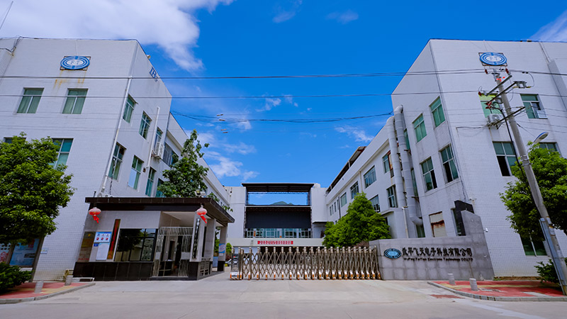
One factory, one quality system, three decades of practice.
We operate three owned production buildings totalling 15,000 m², staffed by more than 200 skilled operators and engineers under a stable management team. Production runs on industry-standard equipment — LDI imaging, VCP plating, AOI and AVI inspection — with an in-house lab for impedance, network analysis and ion-contamination testing.
Our boards serve AI and computing systems, automotive electronics, telecom and optical modules, aerospace, medical and home-appliance OEMs. Beyond the domestic market, we ship to Europe, the Americas, Japan, Korea and Southeast Asia.
Quality is not a slogan here — it is a set of audited systems: ISO 9001, IATF 16949, UL, ISO 14001, GJB 9001C and CQC, maintained and renewed on schedule.
Quick facts
- Founded1997
- Registered capitalRMB 30 million
- Facility15,000 m² · 3 buildings
- Capacity50,000 m² / month
- Models per month1,200
- Staff200+
- LocationWuping, Fujian, China
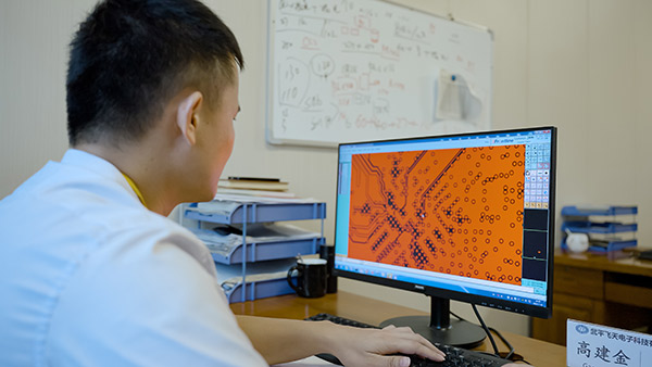
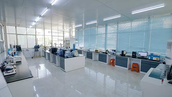
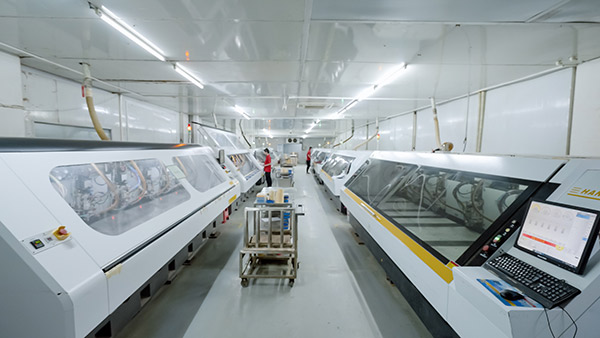
Two minutes on the floor.
Lamination, LDI imaging, plating, AOI and final test — filmed in the same buildings your boards run through. No stock footage, no renderings.
Nearly thirty years, one direction.
Company founded
Feitian Electronics established with an ISO 9001 quality system in place from day one. Capacity: 6,000 m² per month.
Joined SPCA
Admitted to the Shanghai PCB industry association; capacity reached 8,000 m² per month.
Relocated to Wuping Yanqian
Moved into the purpose-built plant in the Yanqian industrial zone; capacity 12,000 m² per month.
Audited by telecom equipment makers
Passed the quality system audits of Huawei and ZTE; capacity 25,000 m² per month.
IATF 16949 & ISO 14001
Certified to ISO 14001 and ISO/TS 16949 (now IATF 16949); capacity 45,000 m² per month.
5G product line
Opened a dedicated 5G product line; facility expanded to 14,500 m² across the current buildings.
Capacity figures above are historical milestones. Current published capacity is 50,000 m² per month.
Where our boards end up.
AI and computing systems
High-layer-count boards for servers, acceleration cards and industrial compute platforms.
Automotive electronics
Antenna, radar and control boards under IATF 16949 process control with lot traceability.
Telecom & optical modules
5G antenna boards, RF front-ends and optical module boards with segmented gold fingers.
Aerospace & satellite
PTFE satellite antenna boards and low-loss RF structures, built under military-standard quality control.
Medical devices
Control, imaging and monitoring boards with full documentation and material traceability.
Appliances & industrial control
Cost-optimised rigid boards for high-volume appliance and automation applications.
Four words we actually use.
See the floor for yourself.
Request the factory audit pack, book a video audit, or simply send a Gerber and let the DFM review speak for us.