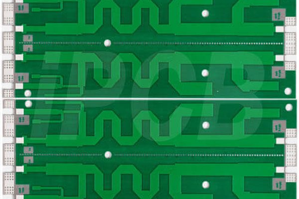
Feed network for satellite antenna arrays on PTFE laminate. Low loss at Ku band, phase-length matching held across the panel by imaging on the same LDI line.
High Frequency PCB
PTFE Antenna Feed Network
2L · PTFE (Dk 2.2) · ±0.1 mm
Technical specifications
Build parameters for this board.
| Layers | 2 |
| Laminate | PTFE (Dk 2.2) |
| Phase match | ±0.1 mm |
| Min trace | 4 / 4 mil |
| Surface finish | Immersion silver |
Catalogue
Other boards on this line
No obligation
Send the file. Get a real answer.
Upload a Gerber and we will come back within 24 hours with the DFM issues, a price and a lead time. If your design is not a fit for our process, we will say so.