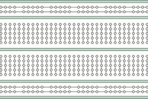
A breadboard is a solderless grid on a 2.54 mm pitch: spring contacts under the holes, power rails along the edges, no heat, no commitment. For validating logic, trying a different op-amp or teaching — it is still the fastest tool in electronics. Nothing here argues against it. The argument is about the boundary.
Four gaps between the demo and the product
| Breadboard | Production PCB | |
|---|---|---|
| Connection | Spring clips: contact resistance is unstable and degrades with vibration and time | Etched copper plus solder: a metallurgical joint with repeatable resistance |
| Electrical behaviour | Uncontrolled parasitics — practical below ~10 MHz only | Controlled impedance, differential pairs, planes; into the tens of GHz with the right stackup |
| Current & environment | Roughly under 200 mA per contact; no tolerance for heat, humidity or vibration | Heavy copper, wide traces, proper base materials, coatings and thermal design |
| Lifecycle | A demo tool, disassembled after the experiment | The physical foundation of a product, manufactured repeatedly for years |
The electrical row is the one that surprises people. A circuit that “works” at 2 MHz on a breadboard can oscillate, radiate or drop bits on a PCB — not because the PCB is worse, but because the breadboard was hiding parasitics the PCB now forces you to manage deliberately.
The standard path from sketch to mass production
- Validate the concept on the breadboard.
- Move to a soldered prototype board once the concept is confirmed.
- Test close to real operating conditions — real supply, real load, real temperature.
- Design the PCB in dedicated software: schematic, placement, routing, design-rule checks.
- Order prototype samples.
- Test block by block, comparing against the breadboard's known-good behaviour.
- Release to mass production.
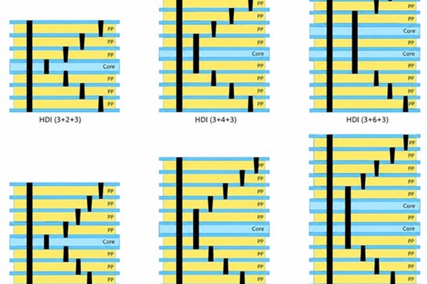
Three layout rules prevent most first-article surprises: keep high-frequency loops small; size trace width and copper to the real current density, not the average; and calculate impedance up front instead of discovering it with an oscilloscope.
If you are the buyer: what to send a fabricator
- A complete requirements package — Gerber plus stackup intent — not a photo of the breadboard.
- Separate pricing for engineering samples, pilot and mass production; they are different processes.
- For automotive, medical or defence work: define traceability and acceptance standards before quoting, not after rework.
And when you move from prototype to production, ask the fabricator to review the stackup before layout freezes. That review is free, and it is where the breadboard's hidden parasitics finally get a cost estimate.
- A breadboard validates logic, not a product: parasitics, current and environment all change on a real PCB.
- Keep the seven-step path honest; skipping the soldered prototype stage is where schedules slip.
- Send the fabricator requirements, not photos — and get the stackup reviewed before layout freezes.