Under IPC-2315 and IPC-4104, a board is HDI only when three things are true at once: conductor width and spacing of 0.10 mm or less, microvias of 0.15 mm or less drilled by laser, and interlayer connections built with blind and buried vias on sequentially laminated layers.
The last condition is the one people forget. A board with buried vias is not automatically HDI — the definition needs blind-via plating plus at least one additional lamination cycle. If a fabricator quotes “HDI” without a second press cycle, they are quoting a standard board with a markup.
The build-up ladder
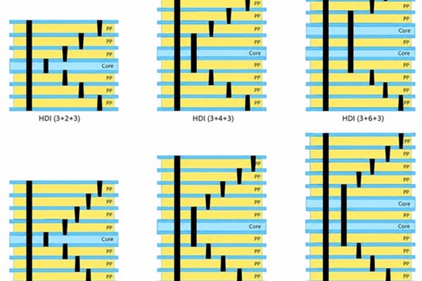
Every HDI board sits on a ladder set by the number of build-up cycles:
- 1+N+1 — one laser-drilled layer pair over a laminated core. The entry point: cost-controlled, and enough for most BGA escapes down to 0.5 mm pitch.
- 2+N+2 — two build-up cycles with staggered or stacked vias. Stacked vias save routing channels but demand clean via-fill plating; this is where most HDI yield problems live.
- 3+N+3 and above — cross-layer drilling for the highest densities: smartphone mainboards, optical modules, medical probes.
We build through 4+N+4 with 0.10 mm laser microvias — everything short of substrate-level IC packaging.
Five differences that decide the quote
| Aspect | Standard multilayer | HDI multilayer |
|---|---|---|
| Structure | Mechanical through-holes, single lamination | Laser microvias, blind/buried vias, sequential lamination |
| Materials | FR-4 across the stack | FR-4 cores with RCC or low-loss prepreg outside; high-end builds use Tg 170 laminates such as S1000-2M |
| Density | 6/6 mil line/space is a comfortable limit | 3/3 mil line/space, 0.10 mm laser vias, via-in-pad |
| Cost behaviour | Cost rises with layer count | Cost rises with build-up order — but density can delete layers, so past ~8 layers HDI often quotes lower than the equivalent standard board |
| Design rules | Connectivity and DFM | +6 mil pad rule on laser vias, ≥9.5 mil edge spacing between blind vias of different nets, filled-and-capped vias |
When HDI pays for itself — and when it does not
The crossover sits around eight layers, but the honest answer depends on why you are there. Choose HDI when the component forces you: 0.4 mm-pitch and finer BGAs, via-in-pad under power pins, or a board the size of a coin. Choose standard multilayer when the constraint is just layer count — six signal layers route comfortably on a standard stack, and the boards are cheaper and faster to build.
Where the middle gets expensive is converting a standard layout to HDI after fan-out has escaped at 6/6 mil. Escapes that barely fit at 6/6 mil will not fit a laser-via pad rule. Catch that at stackup review, not at first article.
What we need from you to quote HDI correctly
- Gerber and a stackup proposal — or just the netlist plus intent, and we propose one.
- Target impedance with tolerance, and which nets carry it.
- Via types per net class: which may be laser, which must be filled, which get thermal reliefs.
- Volume expectation. It changes the tooling answer, not just the price.
Send the files through the upload page and a production engineer — the one who will run the job — replies within 24 hours with a written DFM review, including whether your design genuinely needs HDI.
- HDI is a definition (IPC-2315), not a marketing tier: ≤0.10 mm trace/space, laser microvias, sequential lamination.
- Past roughly eight layers, HDI can cost less than a standard multilayer, because density deletes layers.
- The +6 mil pad rule and the 9.5 mil blind-via spacing are the two rules that break standard-board layouts.