Signal loss through a PCB has three sources: copper, radiation and the dielectric. The first two you fight with geometry. The third you can only buy your way out of — and dielectric loss grows with data rate faster than any geometric fix can chase. Conventional resin systems hold up into the tens of gigabits; by AI-server backplanes, 1.6T optical lines or 224G channels, the resin itself is the bottleneck.
PTFE brings four properties the high-speed world cares about: low dielectric constant (about 2.1 for the pure resin), very low dissipation factor, near-zero water absorption and chemical stability. Lower Df preserves eye height and link margin on long channels — the margin a receiver needs after the signal has crossed traces, vias and connectors.
What it buys you — and where it does not
The mistake we see is treating PTFE as a whole-board decision. It rarely is. The channels that need it are the most signal-sensitive ones: the SerDes lanes, the RF runs, the clocks. Everything else is paying PTFE prices for nothing.
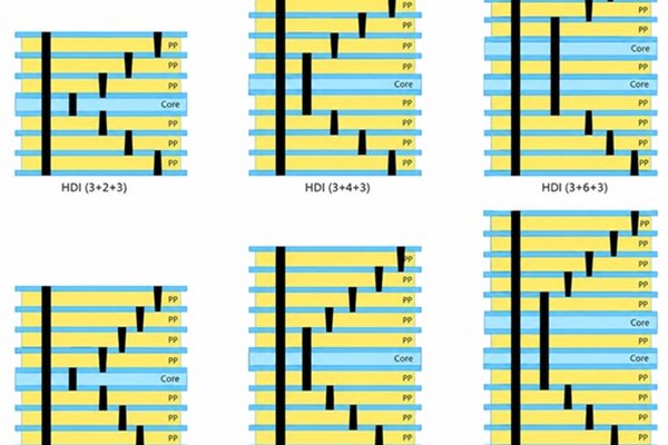
That is why hybrid stackups exist: PTFE or another low-loss laminate on the signal layers, FR-4 everywhere else. Mixed-dielectric lamination is routine work for us — hybrid laminate boards are one of our nine production families — and it keeps the bill of materials honest: you buy low-loss only where the signal path demands it.
Why PTFE is hard to build
Three properties make PTFE difficult, and all three show up in the quote:
- Adhesion. PTFE's low surface energy — the same property that makes it non-stick in a pan — makes copper and epoxy refuse to bond. It needs specialised surface treatment and lamination cycles.
- Mechanical stability. Pure PTFE is soft and expands more than FR-4 with heat. Real materials add glass, ceramic or silica fillers to fix rigidity, CTE and dimensional stability — which is why the datasheet matters more than the brand name.
- Drilling and hole preparation. PTFE does not machine like epoxy-glass. Hole-wall cleanliness, desmear and plasma activation decide whether plating adheres; get it wrong and the via is a latent defect, not a visible one.
None of this makes PTFE exotic. It makes it a process discipline: plasma activation, controlled lamination pressure profiles, TDR impedance verification per lot. Ask any fabricator quoting a PTFE board how they verify impedance — if the answer is not a coupon test with a report, keep walking.
What this means for your quote
- Send the target frequency or data rate, not just “high-speed” — the material choice falls out of the loss budget.
- Ask for hybrid pricing. A PTFE-only stack is almost always the wrong answer economically.
- Impedance tolerance ±5% or better, verified by TDR and reported per lot — the same report ships with the boards.
Upload your Gerber and stackup intent through the upload page: we will come back within 24 hours with a material recommendation and the DFM notes specific to PTFE processing.
- Dielectric loss scales with data rate; geometry fixes stop scaling before 224G does.
- Use PTFE on the sensitive channels and FR-4 on the rest — hybrid stackups keep cost proportional.
- The build risk sits in surface energy and hole-wall prep, and both are testable: demand TDR coupons.