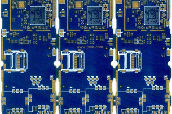
Two stacked micro-via layers per side in blue mask. Stacking registration and copper-filled via integrity are the two yield drivers — both are SPC-monitored on this line.
HDI & IC Substrate
2+N+2 Module Board
2+N+2 · 0.12 mm, stacked · 8–10 total
Technical specifications
Build parameters for this board.
| Build-up | 2+N+2 |
| Micro via | 0.12 mm, stacked |
| Layers | 8–10 total |
| Min trace | 2.5 / 2.5 mil |
| Surface finish | ENEPIG |
Catalogue
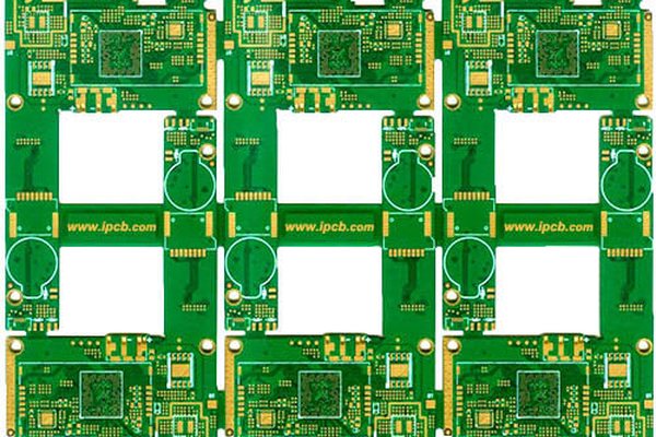
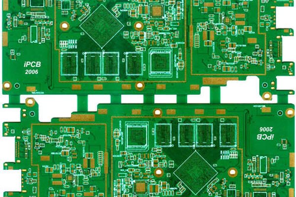
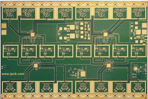
Other boards on this line
No obligation
Send the file. Get a real answer.
Upload a Gerber and we will come back within 24 hours with the DFM issues, a price and a lead time. If your design is not a fit for our process, we will say so.